In the unforgiving landscape of industrial applications—from renewable energy converters to heavy machinery control systems—electronic components are subjected to relentless thermal stress, high electrical loads, and severe mechanical vibration. Standard printed circuit boards often represent the weakest link, prone to failure under these extreme conditions. The solution extends beyond simply using a thicker board; it requires a fundamental shift in design and manufacturing philosophy. This is where the strategic integration of heavy copper PCBs becomes a cornerstone of operational resilience.
The true value of these components is not merely in their capacity to handle more current. It lies in a sophisticated interplay of material science, precision manufacturing, and meticulous Design for Manufacturability (DFM). Mastering these elements translates directly into quantifiable gains in long-term reliability, significantly reducing the total cost of ownership (TCO) by minimizing downtime and maintenance cycles.
Heavy Copper PCB Strategy in 4 Core Areas
- Design for Manufacturability (DFM): Emphasizes precision in etching, plating, and solder mask application to prevent common fabrication defects.
- Quantifiable Robustness: Focuses on performance metrics that prove a lower total cost of ownership through enhanced durability and reduced failure rates.
- Strategic Material Selection: Involves choosing substrates like high-Tg FR-4 or Polyimides to withstand specific industrial stresses like extreme temperatures.
- Technical Specification Mastery: Translates copper weight and design features into predictable current capacity, thermal performance, and EMI control.
Mastering Design for Manufacturability (DFM) in Heavy Copper PCB Fabrication for Industrial Settings
Design for Manufacturability is the critical discipline that bridges the gap between a theoretical design and a physically reliable product. For heavy copper PCBs, DFM is not a suggestion but a necessity. The sheer thickness of the copper layers introduces significant challenges in fabrication that, if unaddressed, can undermine the board’s integrity. Precise control over etching and plating processes is fundamental to achieving uniform copper thickness, especially across complex circuit geometries.
Electroplating ensures uniform copper thickness but requires hours-long processes that demand tight process control to avoid under-etching or over-etching.
– Leadsintec Technical Whitepaper, Comprehensive Guide to Heavy Copper PCBs
Innovations in manufacturing have shown that this level of control is achievable, with advanced techniques leading to a remarkable 30% decrease in over-etching defects. This precision ensures that trace widths and spacing meet design specifications, which is vital for consistent electrical performance. Other key DFM considerations include optimizing thermal relief pads to effectively balance high current distribution with solder joint integrity, a task that becomes exponentially more complex with extreme copper weights.
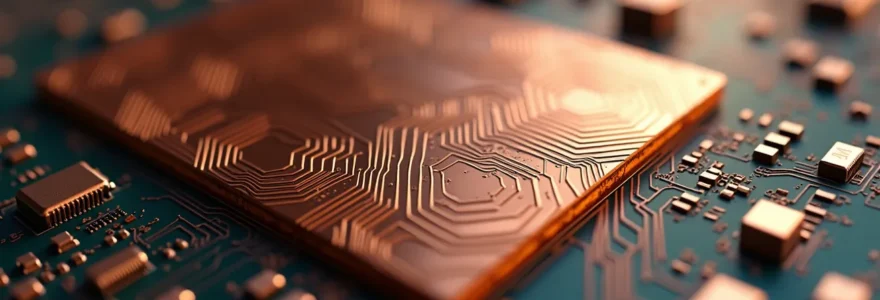
The image below illustrates the intricate results of a well-managed etching process on a heavy copper board. The uniformity and sharp definition of the traces are direct outcomes of a robust DFM strategy, preventing issues like current leakage or hotspots.
Furthermore, solder mask application over these thick layers presents its own set of challenges. Inadequate coverage can lead to solder bridging and short circuits, while poor adhesion can result in delamination over the product’s lifespan. Mitigating these risks requires careful material selection and application techniques tailored specifically to heavy copper topography.
Optimizing Heavy Copper PCB DFM Steps
- Step 1: Select high-Tg substrates to avoid deformation during thick copper processing.
- Step 2: Use partial etching methods to control copper thickness and avoid trace damage.
- Step 3: Optimize thermal relief pads to balance current load and thermal dissipation.
- Step 4: Select solder mask formulations compatible with thick copper to prevent delamination.
Quantifying Robustness: Performance Metrics and Total Cost of Ownership for Industrial Heavy Copper PCBs
The decision to invest in heavy copper PCBs is best understood through tangible performance metrics and a clear analysis of total cost of ownership. While the initial material cost is higher, the long-term financial and operational benefits are substantial. These boards are specifically engineered to prevent common failure modes seen in standard PCBs, such as trace burnout from high currents and delamination due to thermal cycling.
How much more reliable are heavy copper PCBs?
By effectively managing thermal and mechanical stresses, heavy copper designs can reduce failure rates by over 20% in harsh industrial applications, leading to extended equipment lifespan and lower warranty claims.
Establishing clear benchmarks for mechanical stress, vibration resistance, and thermal shock cycles reveals the superior resilience of heavy copper. The following table provides a direct comparison of key performance metrics between heavy copper and standard PCBs, highlighting the profound differences in capability.
| Metric | Heavy Copper PCB | Standard PCB |
|---|---|---|
| Current-Carrying Capacity | Up to 200 A/channel | Below 10 A/channel |
| Thermal Resistance | Low (better dissipation) | High (heat buildup) |
| Mechanical Strength | High resistance to vibration and thermal cycling | Lower durability |
| Warranty Claim Reduction | Over 20% | Baseline |
This enhanced durability translates directly into economic advantages. Reduced warranty claims, extended operational uptime, and fewer maintenance interventions contribute to a significantly lower TCO over the equipment’s lifecycle. As one industrial equipment manufacturer noted, their heavy copper PCB implementation in power controllers cut repair incidents dramatically and confirmed the value of this technology in demanding environments.
Heavy Copper PCB in Wind Turbine Control Systems
A wind turbine control system using heavy copper PCBs experienced three times the lifespan of standard PCBs, reducing maintenance costs by 40% over five years due to enhanced thermal and mechanical durability.
Strategic Material Selection and Manufacturing Nuances for Demanding Industrial Environments
The foundation of a durable heavy copper PCB is its base material. The choice of substrate is a strategic decision that directly impacts the board’s ability to withstand specific industrial challenges, including extreme temperatures, chemical exposure, and high vibration. Advanced material properties such as a high glass transition temperature (Tg), low coefficient of thermal expansion (CTE), and high thermal conductivity are paramount.
A comparison of common base materials reveals distinct advantages for different applications. While high-Tg FR-4 is a cost-effective choice for general industrial use, more demanding environments may necessitate materials like Rogers for high-frequency signals or Polyimides for applications involving extreme temperature fluctuations.
| Material | Dielectric Loss | Thermal Conductivity | Mechanical Integrity | Typical Use |
|---|---|---|---|---|
| FR-4 (High Tg) | Moderate | Low to Moderate | Good | General Industrial |
| Rogers | Low | Moderate | Good | High-Frequency, High-Reliability |
| Polyimides | Low | High | Excellent | Extreme Temp, Aerospace |
| Ceramic | Very Low | Very High | Excellent | High Power, Thermal Management |
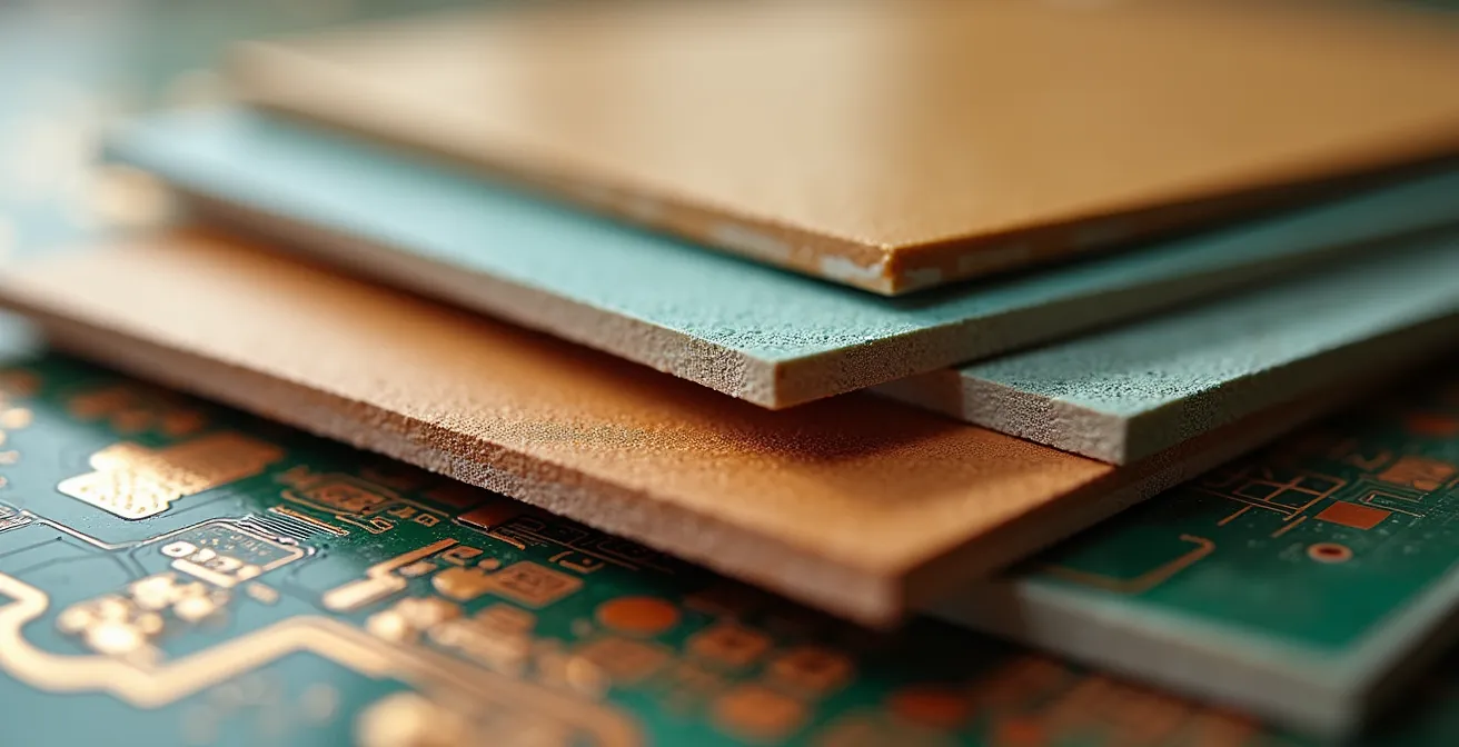
The image below provides a conceptual look at the variety of substrate materials available. Each layer possesses unique thermal and mechanical properties, and the right selection is crucial for creating a board that will not fail under stress.
Beyond material selection, advanced manufacturing techniques such as selective copper deposition or specialized lamination processes for ultra-thick layers are often required. As noted by manufacturing experts, composite substrates combined with these advanced techniques are critical for maintaining both electrical and mechanical reliability. Establishing and adhering to critical manufacturing tolerances is the final piece of the puzzle, directly impacting electrical performance, thermal dissipation, and overall board integrity.
Key Manufacturing Tolerances for Heavy Copper PCB
- Maintain copper thickness uniformity within ±10%
- Control via plating thickness to ensure current and thermal capacity
- Limit line width variation to ±5%
- Use thermal shock testing to validate substrate performance
Key Takeaways
- DFM is paramount for reliability, directly impacting etching precision and solder mask integrity on thick copper.
- The true value lies in lower Total Cost of Ownership (TCO) through reduced failures and extended equipment lifespan.
- Strategic material selection (High-Tg FR-4, Rogers) is critical for matching performance to specific industrial stresses.
- Properly engineered heavy copper PCBs inherently improve thermal management and mitigate EMI, boosting system stability.
Translating Technical Specifications: Current Capacity, Thermal Performance, and EMI/EMC Management
Understanding the technical specifications of a heavy copper PCB is key to leveraging its full potential. The most fundamental specification is the conversion of copper weight (measured in ounces) to its current-carrying capacity. However, simply reading a chart is insufficient for industrial design; derating factors must be applied to account for operating temperatures and board complexity.
The thermal resistance of thick copper layers and vias is another critical parameter. Lower thermal resistance means heat generated by components is dissipated more effectively, which directly extends component lifespan and improves overall system stability. This is particularly crucial for high-power printed circuit boards where thermal runaway is a significant risk.
| Copper Weight (oz) | Typical Current Capacity (A) at 1mm Width | Thermal Resistance Impact | Derating Factor for Industrial Use |
|---|---|---|---|
| 1 oz | 3 A | Baseline | 1.0 |
| 4 oz | 8-10 A | ~30% lower resistance | 0.85 |
| 10 oz | >20 A | 50% lower resistance | 0.75 |
Finally, managing electromagnetic interference (EMI) and ensuring electromagnetic compatibility (EMC) is vital in high-power systems. The inherent structure of heavy copper PCBs, with their thick power and ground planes, provides excellent natural shielding. This is corroborated by feedback from industrial automation engineers, who report that incorporating these boards resulted in a significant drop in operating temperatures and a near elimination of EMI-related faults. When combined with best practices, you can ensure high quality products that are both powerful and electromagnetically quiet.
Best Practices for EMI/EMC in Heavy Copper PCBs
- Implement proper grounding planes with thick copper layers.
- Use controlled impedance traces to minimize signal reflections.
- Apply EMI shielding strategies such as copper pours and Faraday cages.
- Design vias and plating thickness to handle thermal and current loads effectively.
Frequently Asked Questions on Industrial PCB Technology
What is the primary advantage of heavy copper PCBs over standard ones?
Their main advantages are a significantly higher current-carrying capacity and superior thermal dissipation. This combination leads to far greater durability and reliability in harsh industrial environments where heat and electrical load are major failure factors.
How does copper weight (in oz) affect PCB performance?
Higher copper weight directly increases the cross-sectional area of traces, which boosts current-carrying capacity and reduces thermal resistance. This allows components to run cooler and more reliably under high-power conditions.
Is Design for Manufacturability (DFM) more critical for heavy copper PCBs?
Absolutely. The unique challenges of uniformly etching, plating, and applying solder mask over thick copper layers require precise process controls. A robust DFM strategy is essential to prevent manufacturing defects and ensure long-term operational reliability.
Do heavy copper PCBs help with EMI/EMC issues?
Yes, the thick copper used for ground and power planes provides excellent natural shielding. This helps reduce electromagnetic interference (EMI) and improves the overall electromagnetic compatibility (EMC) of the system, which is critical in high-power industrial electronics.